Extreme ultraviolet (“EUV”) lithography is currently forecasted by the International Technology Roadmap for Semiconductors (“ITRS”) to be the next critical dimension imaging solution after ArF immersion lithography and double patterning extensions. Some forms of memory devices, such as NAND Flash, may need this manufacturing technology after 32nm node devices.
We believe the availability of a high power source for 13.5nm radiation is one of the technologies requiring significant developments to enable the realization of EUV lithography. Other technologies that are needed to enable EUV photolithography include photoresist and mask. Photoresist performance parameters needing the greatest amount of development include sensitivity or speed, line-edge-roughness, and line-width-roughness. Photoresist sensitivity and scanner optical transmission are the basis to derive EUV source power requirements within a usable bandwidth.
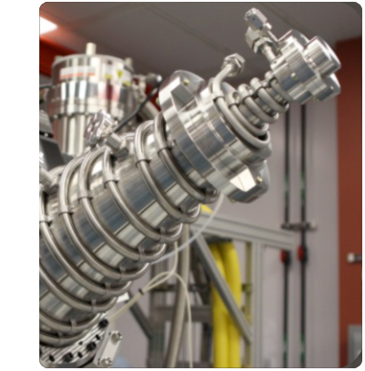
Our laser-produced plasma EUV source system produces 13.5nm radiation and is intended to provide a power source for EUV lithography. As currently configured, it consists of a carbon dioxide laser, a beam transport system, and a plasma chamber. The chamber contains a mirror which collects the emitted light and reimages the plasma source to the intermediate focus position at the entrance to the scanner system. The source plasma chamber is directly coupled to the scanner vacuum chamber and inside the scanner enclosure. We shipped our first EUV prototype source system to ASML in 2009, and expect to record our first sale of an EUV pilot source system to ASML during 2010.