Deep Ultraviolet
Our DUV light sources include the most advanced ArF immersion light sources for use
on the most critical process layers. Chipmakers also use our ArF and KrF light sources
to fill out or balance their production lines or add capacity to their manufacturing
facilities (also referred to as “fabs”) for less critical layers.
The extremely short wavelengths and highly narrowed bandwidths of our light sources
work in concert with our lithography customers’ steppers and scanners and their
sophisticated lens systems to help enable the very fine feature resolution required
for patterning today’s most advanced semiconductor circuitry. In addition, the pulse
energy and repetition rate of our light sources enable our chipmaker customers to
achieve high throughput in wafer processing. We have designed our light sources to be
reliable, easy to install and compatible with existing semiconductor manufacturing
processes. Additionally, we offer focus drilling technology for certain of our ArF
immersion light sources. Focus drilling provides up to two times improvement in the
depth of focus on the wafer, which can positively impact chipmakers’ yield.
In addition to our current DUV product portfolio of light sources, we have numerous models of ArF and KrF light sources that have been superseded and are no longer in active production. However, these systems are still widely used by our customers and make up a substantial portion of our installed base of light sources. We continue to provide installed base products and maintain parts inventory for these systems.
 XLR Series
XLR Series—193 nm ArF Immersion Light Sources
As chipmakers continue to reduce the feature sizes and shrink CDs on the wafer, they
need to install the advanced tools required to enable patterning of the most critical
layers. NAND flash memory and DRAM semiconductor manufacturers have been the most
aggressive chipmakers in shrinking CDs, and have been driving demand for our most
advanced light sources for ArF immersion lithography applications. DRAM manufacturers
are in production with CDs at 45 nm. Currently, some chipmakers are in development of
chip production with CDs of less than 32 nm. Leading edge semiconductor manufacturers
in the memory, logic and foundry sectors have been developing ArF immersion extension
down to CDs of 22 nm and implementing double-patterning technique, which means the
increased demand for ArF immersion light sources could last for several years. The
XLR Series is based on our dual discharge chamber master oscillator power amplifier
(“MOPA”) light source architecture, with a regenerative ring amplifier in place of the
traditional power amplifier. Built on our XL universal platform, this product series
offers a step function improvement in performance and cost of operation. Our XLR light
sources are designed to enable our chipmaker customers to customize performance for
specific applications through improved performance parameters and metrology options.
Flexible power up to 90 watts (“W”), improved bandwidth stability and dose control
enable higher CD control and yield, and this series offers longer pulse duration to
extend the lifetime of the illuminator and lens, even at higher power levels. Cost of
operation is reduced significantly through optical design and component robustness,
leading to increased module lifetime. With active bandwidth stabilization and tuning
capability, the XLR light sources offer improved bandwidth management for improved
mask optical proximity correction matching and tool-to-tool matching, so customers can
use multiple node mask sets in the same tool or the same mask in different tools. We
sell primarily the XLR 600ix model of this series.
 XLA Series
XLA Series—193 nm ArF Dry Light Sources
Though no longer considered leading edge technology, dry ArF lithography is still used
to pattern a significant number of less-critical layers on wafers. Additionally, as CDs
continue to shrink and drive demand for even finer resolution on the most critical
layers, non-critical layers may be patterned with ArF dry scanners, which drives
continued demand for these tools. Our XLA Series of ArF light sources was the
first product series to be based on our dual-discharge chamber MOPA architecture.
MOPA represented a paradigm shift in excimer laser architecture when it was introduced
in 2003. The master oscillator creates a narrow bandwidth beam of light at low power.
The beam then is directed into the power amplifier, where the power is increased
significantly while maintaining the narrow bandwidth. This combination of bandwidth
and power enabled our chipmaker customers to continue reducing CDs and increasing
processing speeds, capacity and functionality of chips, while giving them the
performance and cost advantages they need. Each product in the XLA Series is based
on the XL universal platform, and we continue to sell the XLA 105 model of this series.
 ELS 7010
ELS 7010—248 nm KrF Dry Light Sources
We have been providing KrF light sources for volume chip production since 1996,
when chipmakers required the adoption of DUV light sources in their fabs. Over the
years, we have developed and sold a variety of increasingly powerful and productive
KrF light sources. The 7000 Series is the first series that was designed and built
on a common platform, enabling chipmakers to easily utilize the 193 nm wavelength
produced by ArF and the 248 nm wavelength produced by KrF within the manufacturing
environment. This “ease of use” feature was very important at the time because
chipmakers were introducing ArF production into their fabs and the common platform
simplified the introduction of this new technology. With a 4 kHz repetition rate and
high output power, the 7000 Series provides our chipmaker customers with high wafer
throughput and lower cost of operation by reason of advanced design and materials,
and delivers a high level of tool availability to enable manufacturing efficiency and
flexibility. Our bestselling light source of the series, the ELS-7010 is still in
demand as chipmakers continue to prefer the higher power and narrower bandwidth offered
by this system. In 2010, we introduced the ELS-7010x which allows customers to easily
adjust power from 30 watts to 50 watts based on the changing wafer design requirements
and production needs.
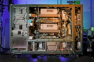
 EUV 3300 Source
Extreme Ultraviolet
Chipmaker demand for EUV light sources continues to be strong, as we believe EUV technology
is the best path toward enabling Moore’s Law and scaling of semiconductors with features 22 nm
wide or smaller. We have accelerated our rate of EUV source development, and are continuing to
increase our investment in development resources, manufacturing capacity, and field support to
fulfill EUV source demand.
Our Laser-Produced Plasma (“LPP”) EUV light source is designed to provide scalable power that enables high volume manufacturing. Our LPP EUV source system consists of a high power, high repetition rate pulsed carbon dioxide laser, a beam delivery system, and a plasma vacuum vessel. The plasma vacuum vessel is complete with a droplet generator and collector, debris mitigation, and in-situ metrology to measure, monitor and control the system operation. The 13.5 nm wavelength is produced when a carbon dioxide laser pulse strikes small droplets of elemental tin in the plasma chamber. The laser heats the droplet of tin to the point of evaporation and super-heating to critical temperature, then the atoms shed their electrons and become highly ionized (i.e., a plasma). This causes the excited tin ions (the plasma) to emit light which is collected by a highly reflective mirror. The mirror reflects and directs the resulting 13.5 nm wavelength energy and focuses it through an aperture and into the lithography system. The plasma chamber of the EUV source is directly coupled to the scanner system’s vacuum chamber inside the scanner enclosure, requiring close coordination between the designs of our EUV source and the scanner produced by the lithography tool manufacturer. We are working closely with ASML, a lithography tool manufacturer and current customer for our EUV sources, and our key suppliers to drive execution to our power and performance roadmap. Our EUV sources are still under development and not yet capable of supporting the commercial production of integrated circuits; however, we have shipped six EUV 3100 pilot sources to date and, in 2011, we received customer acceptance and recorded revenue for three of these sources. We also received orders for our next generation EUV 3300 sources, which we expect to start shipping in 2012.